Innovations in semiconductor materials have enabled many recent advances in technology from cell phones to flat panel displays to solid state lighting to solar electricity. All of these applications make use of thin layers of semiconductors on the order of a micron thick and most require semiconductors that are crystalline and aligned with a single crystal substrate.
There are great opportunities for further advances in semiconductor materials and new physical phenomena, as well as important unmet needs for new technology. We are exploring the growth of III-V compound semiconductors and oxide materials on single crystal substrates using molecular beam epitaxy ("MBE"), and studying their electronic and optical properties.
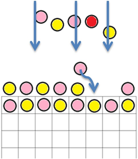
MBE is a method for growing thin crystalline layers in high vacuum using beams of atoms produced by heated effusion cells. The atom fluxes can be controlled with mechanical shutters so that only a fraction of an atomic layer is deposited at a time. By assembling materials from beams of atoms on a temperature-controlled single-crystal template we are able to make novel metastable materials, that have new and useful properties, that cannot be made in bulk form. In the self-assembly process that occurs during crystal growth by vapour deposition of atoms onto a surface, characteristic macroscopic patterns develop as the thickness of the deposited layer grows. These macroscopic patterns develop from atomic scale phenomena and can in some cases be described mathematically. A primary focus of our program is the growth of III-V compound semiconductors and rare earth doped oxides for light emitting devices for medical diagnostics and therapy.
Home
Research
Publication
People
MBE wiki
Links
Research
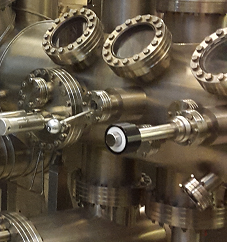
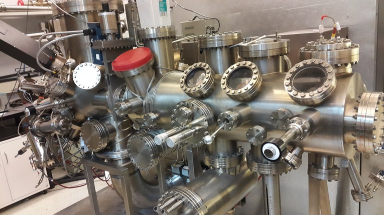
UVic's Molecular Beam Epitaxy system
Substrate
Crystal growth
Atomic Beam
Theme designed by Vahid bahrami Yekta (c) 2016